- 您现在的位置:买卖IC网 > Sheet目录312 > AT25F1024AN-10SU-2.7 (Atmel)IC FLASH 1MBIT 33MHZ 8SOIC
�� �
�
�AT25F1024A�
�The� Ready/Busy� status� of� the� device� can� be� determined� by� initiating� a� RDSR� instruction.� If� Bit� 0�
�=� 1,� the� program� cycle� is� still� in� progress.� If� Bit� 0� =� 0,� the� program� cycle� has� ended.� Only� the�
�RDSR� instruction� is� enabled� during� the� program� cycle.�
�A� single� Program� instruction� programs� 1� to� 256� consecutive� bytes� within� a� page� if� it� is� not� write�
�protected.� The� starting� byte� could� be� anywhere� within� the� page.� When� the� end� of� the� page� is�
�reached,� the� address� will� wrap� around� to� the� beginning� of� the� same� page.� If� the� data� to� be� pro-�
�grammed� are� less� than� a� full� page,� the� data� of� all� other� bytes� on� the� same� page� will� remain�
�unchanged.� If� more� than� 256� bytes� of� data� are� provided,� the� address� counter� will� roll� over� on� the�
�same� page� and� the� previous� data� provided� will� be� replaced.� The� same� byte� cannot� be� repro-�
�grammed� without� erasing� the� whole� sector� first.� The� AT25F1024A� will� automatically� return� to� the�
�write� disable� state� at� the� completion� of� the� Program� cycle.�
�Note:�
�If� the� device� is� not� write� enabled� (WREN),� the� device� will� ignore� the� Write� instruction� and� will�
�return� to� the� standby� state,� when� CS� is� brought� high.� A� new� CS� falling� edge� is� required� to� re-ini-�
�tiate� the� serial� communication.�
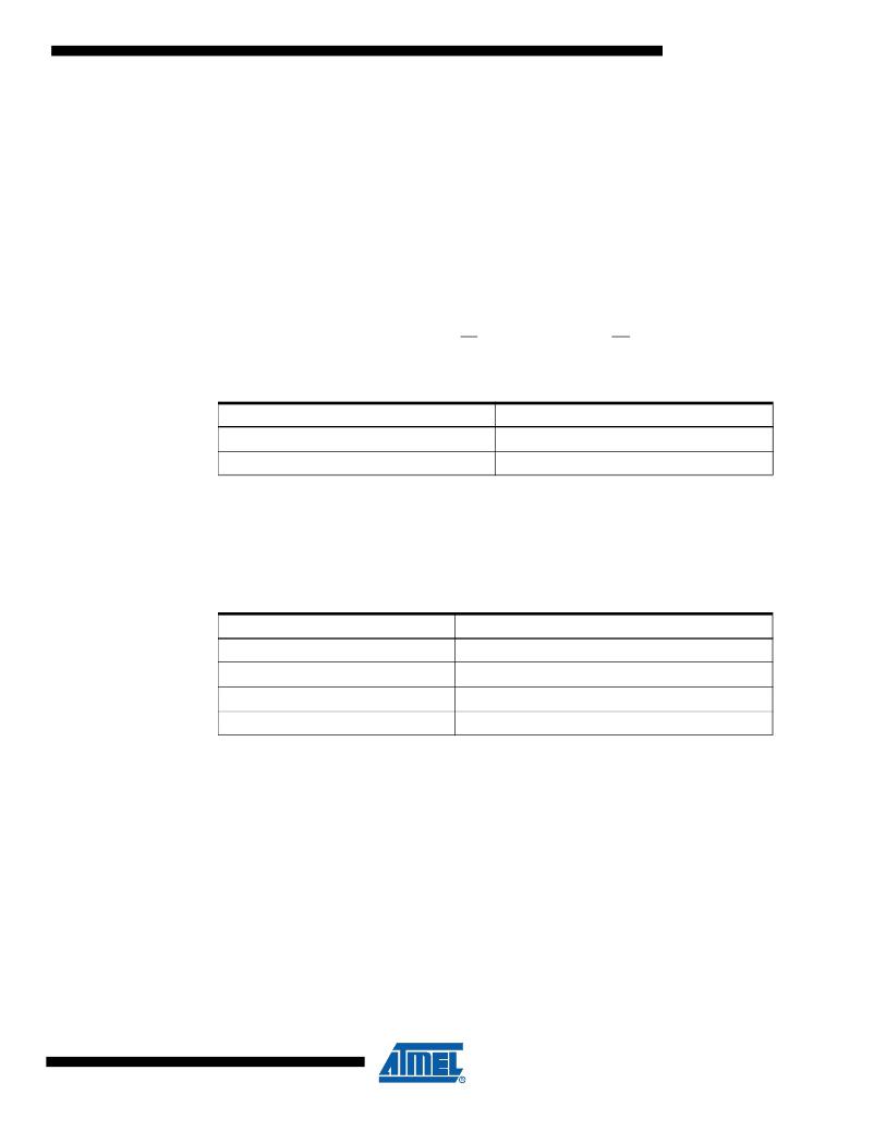
�Table� 2-6.�
�Address� Key�
�Address�
�A� N�
�Don’t� Care� Bits�
�AT25F1024A�
�A� 16� –� A� 0�
�A� 23� –� A� 17�
�SECTOR� ERASE� (SECTOR� ERASE):� Before� a� byte� can� be� reprogrammed,� the� sector� which�
�contains� the� byte� must� be� erased.� In� order� to� erase� the� AT25F1024A,� two� separate� instructions�
�must� be� executed.� First,� the� device� must� be� write� enabled� via� the� WREN� instruction.� Then� the�
�Sector� Erase� instruction� can� be� executed.�
�Table� 1.� Sector� Addresses�
�Sector� Address�
�000000� to� 007FFF�
�008000� to� 00FFFF�
�010000� to� 017FFF�
�018000� to� 01FFFF�
�AT25F1024A� Sector�
�Sector� 1�
�Sector� 2�
�Sector� 3�
�Sector� 4�
�The� Sector� Erase� instruction� erases� every� byte� in� the� selected� sector� if� the� sector� is� not� locked�
�out.� Sector� address� is� automatically� determined� if� any� address� within� the� sector� is� selected.� The�
�Sector� Erase� instruction� is� internally� controlled;� it� will� automatically� be� timed� to� completion.� Dur-�
�ing� this� time,� all� commands� will� be� ignored,� except� RDSR� instruction.� The� AT25F1024A� will�
�automatically� return� to� the� write� disable� state� at� the� completion� of� the� Sector� Erase� cycle.�
�CHIP� ERASE� (CHIP� ERASE):� As� an� alternative� to� the� Sector� Erase,� the� Chip� Erase� instruction�
�will� erase� every� byte� in� all� sectors� that� are� not� locked� out.� First,� the� device� must� be� write� enabled�
�via� the� WREN� instruction.� Then� the� Chip� Erase� instruction� can� be� executed.� The� Chip� Erase�
�instruction� is� internally� controlled;� it� will� automatically� be� timed� to� completion.� The� Chip� Erase�
�cycle� time� typically� is� 3.5� seconds.� During� the� internal� erase� cycle,� all� instructions� will� be� ignored�
�except� RDSR.� The� AT25F1024A� will� automatically� return� to� the� write� disable� state� at� the� com-�
�pletion� of� the� Chip� Erase� cycle.�
�11�
�3346G–SFLSH–7/07�
�发布紧急采购,3分钟左右您将得到回复。
相关PDF资料
AT25F2048N-10SU-2.7
IC FLASH 2MBIT 33MHZ 8SOIC
AT25F4096W-10SU-2.7
IC FLASH 4MBIT 33MHZ 8SOIC
AT25HP512W2-10SI-2.7 SL383
IC EEPROM 512KBIT 10MHZ 16SOIC
AT26DF081A-SSU
IC FLASH 8MBIT 70MHZ 8SOIC
AT26DF161-SU
IC FLASH 16MBIT 66MHZ 8SOIC
AT26DF161A-MU
IC FLASH 16MBIT 70MHZ 8QFN
AT26DF321-SU
IC FLASH 32MBIT 66MHZ 8SOIC
AT27BV010-90JU
IC OTP 1MBIT 90NS 32PLCC
相关代理商/技术参数
AT25F1024AY4-10YU-2.7
制造商:ATMEL 制造商全称:ATMEL Corporation 功能描述:1Mbit High Speed SPI Serial Flash Memory 1M (131,072 x 8)
AT25F1024C1-10CC-2.7
制造商:未知厂家 制造商全称:未知厂家 功能描述:SPI Serial EEPROM
AT25F1024C1-10CI-2.7
制造商:未知厂家 制造商全称:未知厂家 功能描述:SPI Serial EEPROM
AT25F1024N-10SI-2.7
制造商:Atmel Corporation 功能描述:Flash Serial-SPI 3V/3.3V 1Mbit 128K x 8bit 20ns 8-Pin SOIC
AT25F1024N-10SU-2.7
制造商:ATMEL 制造商全称:ATMEL Corporation 功能描述:SPI Serial Memory
AT25F1024Y4-10YU-2.7
制造商:ATMEL 制造商全称:ATMEL Corporation 功能描述:SPI Serial Memory
AT25F2048
制造商:ATMEL 制造商全称:ATMEL Corporation 功能描述:SPI Serial Memory 2M (262,144 x 8)
AT25F2048_07
制造商:ATMEL 制造商全称:ATMEL Corporation 功能描述:2Mbit High Speed SPI Serial Flash Memory 2M (262,144 x 8)